Introduction to Script 3
The GUI allows you to set parameters and conditions related to the NAND Flash Memory (NAND) to be measured.
On the other hand, with Script, almost all of these settings can be set individually, so you can change the settings at any time during the test and continue evaluation.
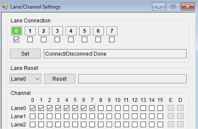
SETCHN Parameter
| Hex 4 digits | Set the channel for measurement using bits |
| LSB:Channel 0, MSB:Channel 15 | |
| In the above figure, 00FF |
By the way, Lane settings cannot be done using Script, so please connect using GUI.
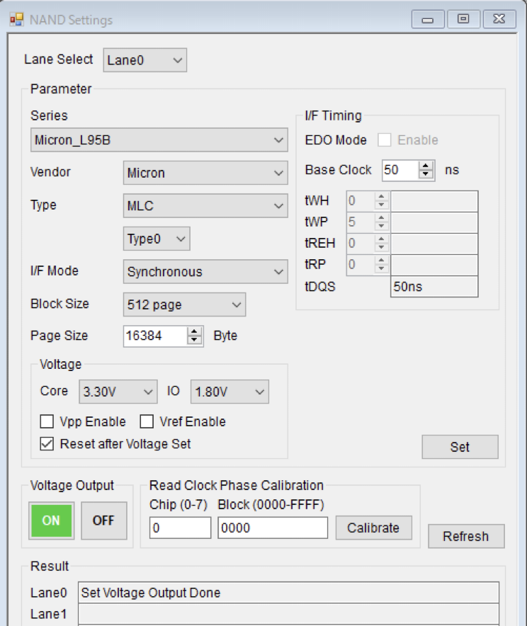
The parameters of NAND Setting shown above can be set using the following commands.
SETPRM Parameter1,2,,,, 17
Parameter
| 1 | Hex 4 digits | Select from the vendors below and set by number | ||||
| 00 | Micron | 03 | Intel | 10 | Other | |
| 01 | Kioxia | 04 | SanDisk | |||
| 02 | Samusung | 05 | Hynix | |||
| 2 | Hex 4 digits | Select from the NAND types below and set the number | ||||
| 0000 | SLC | 0004 | SLC_3D | 0011 | MLC_SLCMODE | |
| 0001 | MLC | 0005 | MLC_3D | 0012 | TLC_SLCMODE | |
| 0002 | TLC | 0006 | TLC_3D | 0015 | MLC_3D_SLCMODE | |
| 0007 | QLC_3D | 0016 | TLC_3D_SLCMODE | |||
| 3 | Hex 2 digits | Subtype: Indicates our unique control mode type. If you are unsure, please contact us. |
| 00 | Type0 | |
| 01 | Type1 | |
| 02 | Type2 | |
| 03 | Type3 |
| 4 | Hex 2 digits | interface mode |
| 00 | Asynchronous | |
| 01 | Synchronous | |
| 02 | ToggleDDR | |
| 03 | NV-DDR2 |
| 5 | Hex 4 digits | Blog size: Number of pages in 1 block |
| 6 | Hex 6 digits | Page size: number of bytes per page |
| 7 | 0 or 1 | EDO mode |
| 0:Disable, 1:Enable | ||
| 8 | Hex 4 digits | Base clock (unit: ns) |
| Asynchronous mode: Set from 10ns to 500ns in 1ns steps | ||
| Modes other than Asynchronous mode: Set from 5ns to 250ns in 1ns steps | ||
| 9 | Hex 2 digits | tWH |
| Asynchronous mode: 00:BCx1, 01:BCx2, …, 0F:BCx16 | ||
| Synchronous mode: Not configurable | ||
| Toggle DDR mode, NV-DDR2 mode: 00:BCx2, 01:BCx4, …, 0F:BCx32 | ||
| 10 | Hex 2 digits | tWP |
| The setting method is the same as parameter 9. | ||
| 11 | Hex 2 digits | tREH |
| Asynchronous mode: 00:BCx1, 01:BCx2, …, 0F:BCx16 | ||
| Modes other than Asynchronous mode: Cannot be set | ||
| 12 | Hex 2 digits | tRP |
| The setting method is the same as parameter 11. | ||
| 13 | Hex 2 digits | Core voltage (set from 0.90V to 3.50V in 0.05V steps) |
| 00:0.9V, 01:0.95V, 02:1.00V, …, 32:3.40V, 33:3.45V, 34:3.50V | ||
| 14 | Hex 2 digits | I/O voltage (set from 0.90V to 3.50V in 0.05V steps) |
| 00:0.9V, 01:0.95V, 02:1.00V, …, 32:3.40V, 33:3.45V, 34:3.50V | ||
| 15 | 0 or 1 | Programming voltage Vpp |
| Valid only when the sub-board is a socket replaceable type. | ||
| Socket fixed type sub-boards are not supported. | ||
| 0:Disable, 1:Enable | ||
| 16 | 0 or 1 | Reference voltage Vref |
| 0:Disable, 1:Enable | ||
| 17 | 0 or 1 | Resetting NAND flash memory after voltage setting |
| 0:Disable, 1:Enable |
In addition, when using an integrated sub-board (introduced on May 13, 2023) that is not a socket-separable (Swappable) type.
For details, please refer to the Operation Guide.
STVOUT Parameter
| 0 or 1 | Whether to output (supply) voltage to NAND |
| This setting is valid when the sub-board is a socket replaceable type. | |
| Socket fixed type sub-boards do not support voltage output control and always output voltage. | |
| 0:Stop, 1:Output |
RCPCAL Parameter1,2
Parameter:Calibrates the read clock phase using the specified block.
| 1 | Hex 2 digits | Chip number |
| 2 | Hex 4 digits | Block number |
As mentioned above, individual settings can be made, so it is also possible to vary the voltage and evaluate its dependence,
If you need a new NAND or additional parameters, please contact us.